- 您现在的位置:买卖IC网 > Sheet目录1999 > ICS87973DYI-147LF (IDT, Integrated Device Technology Inc)IC CLK MULT/ZD BUFFER 52TQFP
ICS87973I-147
LOW SKEW, 1-TO-12, LVCMOS/LVTTL CLOCK MULTIPLIER/ZERO DELAY BUFFER
IDT / ICS LVCMOS CLOCK MULTIPLIER/ZERO DELAY BUFFER
8
ICS87973DYI-147 REV. A DECEMBER 9, 2008
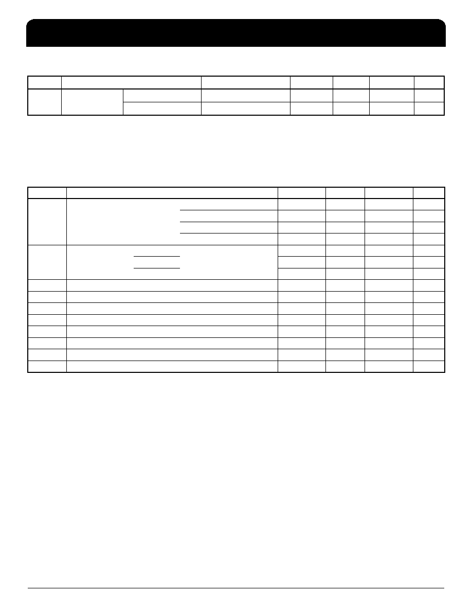
Table 5. Input Frequency Characteristics, VDD = VDDA = VDDO = 3.3V ± 5%, TA = -40°C to 85°C
NOTE 1: Input frequency depends on the feedback divide ratio to ensure "clock * feedback divide" is in the VCO range of 240MHz to
500MHz.
AC Electrical Characteristics
Table 6. AC Characteristics, VDD = VDDA = VDDO = 3.3V ± 5%, TA = -40°C to 85°C
NOTE: Electrical parameters are guaranteed over the specified ambient operating temperature range, which is established when the
device is mounted in a test socket with maintained transverse airflow greater than 500 lfpm. The device will meet specifications after
thermal equilibrium has been reached under these conditions.
NOTE 1: Defined as the time difference between the input reference clock and the average feedback input signal when the PLL is locked
and the input reference frequency is stable.
NOTE 2: Defined as skew between outputs at the same supply voltage and with equal load conditions. Measured at VDDO/2.
NOTE 3: This parameter is defined in accordance with JEDEC Standard 65.
NOTE 4: These parameters are guaranteed by characterization. Not tested in production.
Symbol
Parameter
Test Conditions
Minimum
Typical
Maximum
Units
FIN
Input Frequency
CLK0, CLK1; NOTE 1
120
MHz
FRZ_CLK
20
MHz
Symbol
Parameter
Test Conditions
Minimum
Typical
Maximum
Units
fMAX
Output Frequency
÷2
150
MHz
÷4
125
MHz
÷6
83.33
MHz
÷8
62.5
MHz
t()
Static Phase Offset;
NOTE 1
CLK0
QFB ÷ 8,
In Frequency = 50MHz
-10
145
300
ps
CLK1
-65
90
245
ps
CLK, nCLK
-130
18
165
ps
tsk(o)
Output Skew; NOTE 2, 3
200
ps
tjit(cc)
Cycle-to-Cycle Jitter; NOTE 3
All Banks ÷ 4
55
ps
fVCO
PLL VCO Lock Range
240
500
MHz
tLOCK
PLL Lock Time; NOTE 4
10
ms
tR / tF
Output Rise/Fall Time
0.8V to 2V
150
700
ps
odc
Output Duty Cycle
45
55
%
tPZL, tPZH
Output Enable Time; NOTE 4
10
ns
tPLZL, tPHZ Output Disable Time; NOTE 4
8ns
发布紧急采购,3分钟左右您将得到回复。
相关PDF资料
ICS87973DYILFT
IC CLK MULT/ZD BUFFER 52-LQFP
ICS87974CYILF
IC CLK GEN LVCMOS/LVTTL 52-LQFP
ICS894D115AGI-04LF
IC CLK/DATA RECOVERY 20-TSSOP
ICS894D115BGI-01LF
IC CLK/DATA RECOVERY 20-TSSOP
ICS9112AM-17LF
IC BUFFER HI PERFORMANCE 16-SOIC
ICS91305AMILF
IC CLOCK DRIVER LO JITTER 8-SOIC
ICS91305AMLF
IC CLOCK DRIVER LO JITTER 8-SOIC
ICS91309AGILF
IC CLK BUFFER ZD PLL 16TSSOP
相关代理商/技术参数
ICS87973DYI-147LFT
功能描述:IC CLK MULT/ZD BUFFER 52TQFP RoHS:是 类别:集成电路 (IC) >> 时钟/计时 - 时钟发生器,PLL,频率合成器 系列:HiPerClockS™ 标准包装:1,000 系列:- 类型:时钟/频率合成器,扇出分配 PLL:- 输入:- 输出:- 电路数:- 比率 - 输入:输出:- 差分 - 输入:输出:- 频率 - 最大:- 除法器/乘法器:- 电源电压:- 工作温度:- 安装类型:表面贴装 封装/外壳:56-VFQFN 裸露焊盘 供应商设备封装:56-VFQFP-EP(8x8) 包装:带卷 (TR) 其它名称:844S012AKI-01LFT
ICS87973DYILF
功能描述:IC CLK MULT/ZD BUFFER 52-LQFP RoHS:是 类别:集成电路 (IC) >> 时钟/计时 - 时钟发生器,PLL,频率合成器 系列:HiPerClockS™ 标准包装:2,000 系列:- 类型:PLL 频率合成器 PLL:是 输入:晶体 输出:时钟 电路数:1 比率 - 输入:输出:1:1 差分 - 输入:输出:无/无 频率 - 最大:1GHz 除法器/乘法器:是/无 电源电压:4.5 V ~ 5.5 V 工作温度:-20°C ~ 85°C 安装类型:表面贴装 封装/外壳:16-LSSOP(0.175",4.40mm 宽) 供应商设备封装:16-SSOP 包装:带卷 (TR) 其它名称:NJW1504V-TE1-NDNJW1504V-TE1TR
ICS87973DYILFT
功能描述:IC CLK MULT/ZD BUFFER 52-LQFP RoHS:是 类别:集成电路 (IC) >> 时钟/计时 - 时钟发生器,PLL,频率合成器 系列:HiPerClockS™ 标准包装:1,000 系列:- 类型:时钟/频率合成器,扇出分配 PLL:- 输入:- 输出:- 电路数:- 比率 - 输入:输出:- 差分 - 输入:输出:- 频率 - 最大:- 除法器/乘法器:- 电源电压:- 工作温度:- 安装类型:表面贴装 封装/外壳:56-VFQFN 裸露焊盘 供应商设备封装:56-VFQFP-EP(8x8) 包装:带卷 (TR) 其它名称:844S012AKI-01LFT
ICS87974CYILF
功能描述:IC CLK GEN LVCMOS/LVTTL 52-LQFP RoHS:是 类别:集成电路 (IC) >> 时钟/计时 - 时钟发生器,PLL,频率合成器 系列:HiPerClockS™ 标准包装:1,000 系列:- 类型:时钟/频率合成器,扇出分配 PLL:- 输入:- 输出:- 电路数:- 比率 - 输入:输出:- 差分 - 输入:输出:- 频率 - 最大:- 除法器/乘法器:- 电源电压:- 工作温度:- 安装类型:表面贴装 封装/外壳:56-VFQFN 裸露焊盘 供应商设备封装:56-VFQFP-EP(8x8) 包装:带卷 (TR) 其它名称:844S012AKI-01LFT
ICS87974CYILFT
功能描述:IC CLOCK GEN 1-15 PLL 52-LQFP RoHS:是 类别:集成电路 (IC) >> 时钟/计时 - 时钟发生器,PLL,频率合成器 系列:HiPerClockS™ 标准包装:1,000 系列:- 类型:时钟/频率合成器,扇出分配 PLL:- 输入:- 输出:- 电路数:- 比率 - 输入:输出:- 差分 - 输入:输出:- 频率 - 最大:- 除法器/乘法器:- 电源电压:- 工作温度:- 安装类型:表面贴装 封装/外壳:56-VFQFN 裸露焊盘 供应商设备封装:56-VFQFP-EP(8x8) 包装:带卷 (TR) 其它名称:844S012AKI-01LFT
ICS879893AYILF
功能描述:IC CLK GEN LVCMOS/LVTTL 48-LQFP RoHS:是 类别:集成电路 (IC) >> 时钟/计时 - 时钟发生器,PLL,频率合成器 系列:HiPerClockS™ 标准包装:1,000 系列:- 类型:时钟/频率合成器,扇出分配 PLL:- 输入:- 输出:- 电路数:- 比率 - 输入:输出:- 差分 - 输入:输出:- 频率 - 最大:- 除法器/乘法器:- 电源电压:- 工作温度:- 安装类型:表面贴装 封装/外壳:56-VFQFN 裸露焊盘 供应商设备封装:56-VFQFP-EP(8x8) 包装:带卷 (TR) 其它名称:844S012AKI-01LFT
ICS879893AYILFT
功能描述:IC CLK GEN LVCMOS/LVTTL 48-LQFP RoHS:是 类别:集成电路 (IC) >> 时钟/计时 - 时钟发生器,PLL,频率合成器 系列:HiPerClockS™ 标准包装:1,000 系列:- 类型:时钟/频率合成器,扇出分配 PLL:- 输入:- 输出:- 电路数:- 比率 - 输入:输出:- 差分 - 输入:输出:- 频率 - 最大:- 除法器/乘法器:- 电源电压:- 工作温度:- 安装类型:表面贴装 封装/外壳:56-VFQFN 裸露焊盘 供应商设备封装:56-VFQFP-EP(8x8) 包装:带卷 (TR) 其它名称:844S012AKI-01LFT
ICS87993AYILF
功能描述:IC PLL CLK DRIVER 1-5 32-LQFP RoHS:是 类别:集成电路 (IC) >> 时钟/计时 - 时钟发生器,PLL,频率合成器 系列:HiPerClockS™ 标准包装:1,000 系列:- 类型:时钟/频率合成器,扇出分配 PLL:- 输入:- 输出:- 电路数:- 比率 - 输入:输出:- 差分 - 输入:输出:- 频率 - 最大:- 除法器/乘法器:- 电源电压:- 工作温度:- 安装类型:表面贴装 封装/外壳:56-VFQFN 裸露焊盘 供应商设备封装:56-VFQFP-EP(8x8) 包装:带卷 (TR) 其它名称:844S012AKI-01LFT